- 您现在的位置:买卖IC网 > Sheet目录330 > IDT71V3577S75BQG (IDT, Integrated Device Technology Inc)IC SRAM 4MBIT 75NS 165FBGA
IDT71V3577S_79S, IDT71V3577SA_79SA, 128K x 36, 256K x 18, 3.3V Synchronous SRAMs with
3.3V I/O, Flow-Through Outputs, Burst Counter, Single Cycle Deselect Commercial and Industrial Temperature Ranges
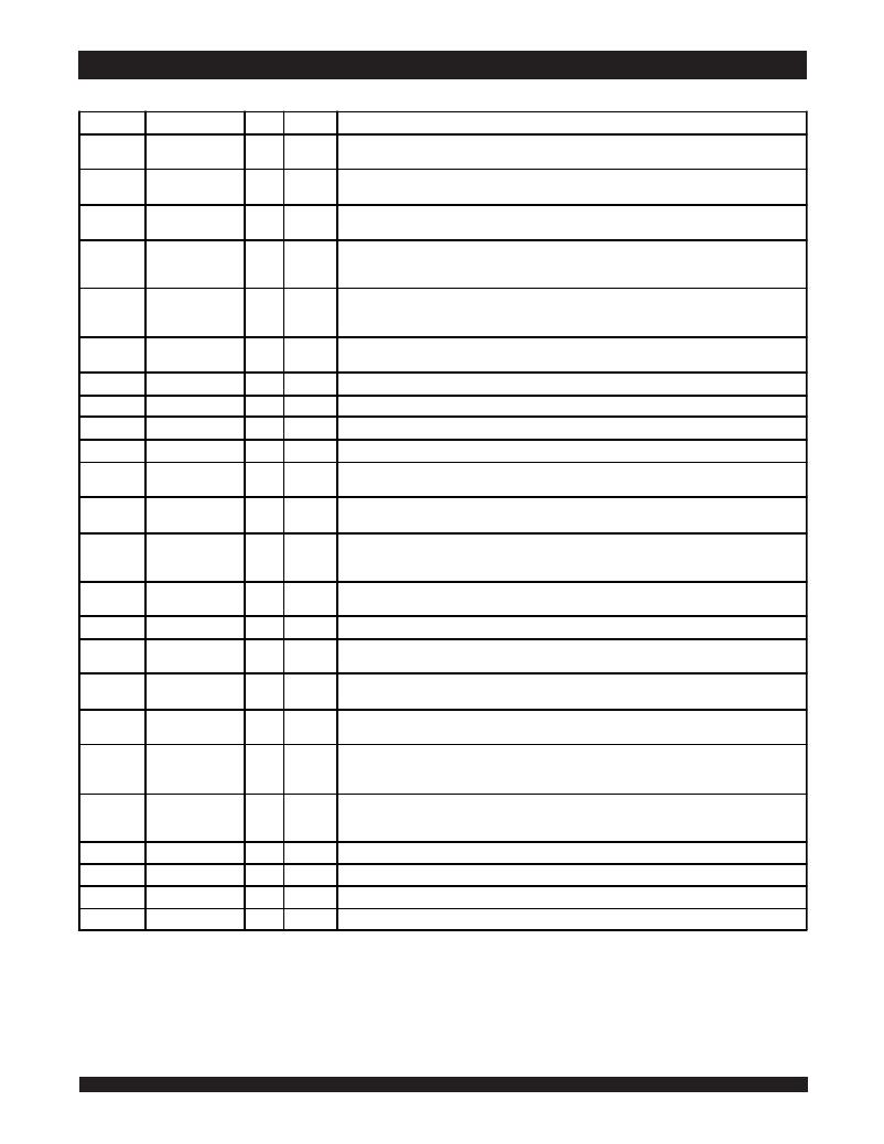
Pin Definitions (1)
Symbol
A 0 -A 17
Pin Function
Address Inputs
I/O
I
Active
N/A
Description
Synchronous Address inputs. The address register is triggered by a combi-nation of the rising edge of CLK
and ADSC Low or ADSP Low and CE Low.
ADSC
Address Status
I
LOW
Synchronous Address Status from Cache Controller. ADSC is an active LOW input that is used to load the
(Cache Controller)
address registers with new addresses.
ADSP
Address Status
I
LOW
Synchronous Address Status from Processor. ADSP is an active LOW input that is used to load the address
(Processor)
registers with new addresses. ADSP is gated by CE .
ADV
Burst Address
I
LOW
Synchronous Address Advance. ADV is an active LOW input that is used to advance the internal burst counter,
Advance
controlling burst access after the initial address is loaded. When the input is HIGH the burst counter is not
incremented; that is, there is no address advance.
BWE
Byte Write Enable
I
LOW
Synchronous byte write enable gates the byte write inputs BW 1 - BW 4 . If BWE is LOW at the rising edge of CLK
then BW x inputs are passed to the next stage in the circuit. If BWE is HIGH then the byte write inputs are
blocked and only GW can initiate a write cycle.
BW 1 - BW 4
Individual Byte
I
LOW
Synchronous byte write enables. BW 1 controls I/O 0-7 , I/O P1 , BW 2 controls I/O 8-15 , I/O P2 , etc. Any active byte
Write Enables
write causes all outputs to be disabled.
CE
CLK
CS 0
CS 1
GW
Chip Enable
Clock
Chip Select 0
Chip Select 1
Global Write
I
I
I
I
I
LOW
N/A
HIGH
LOW
LOW
Synchronous chip enable. CE is used with CS 0 and CS 1 to enable the IDT71V3577/79. CE also gates ADSP .
This is the clock input. All timing references for the device are made with respect to this input.
Synchronous active HIGH chip select. CS 0 is used with CE and CS 1 to enable the chip.
Synchronous active LOW chip select. CS 1 is used with CE and CS 0 to enable the chip.
Synchronous global write enable. This input will write all four 9-bit data bytes when LOW on the rising edge of
Enable
CLK. GW supersedes individual byte write enables.
I/O 0 -I/O 31
Data Input/Output
I/O
N/A
Synchronous data inp ut/output (I/O) pins. The data input path is registered, triggered by the rising edge of
I/O P1 -I/O P4
CLK. The data o utput path is flow-through (no output register).
LBO
Linear Burst Order
I
LOW
Asynchronous b urst order selection input. When LBO is HIGH, the inter-leaved burst sequence is selected.
When LBO is LOW the Linear burst sequence is selected. LBO is a static input and must not change state
while the device is operating.
OE
Output Enable
I
LOW
Asynchronous output enable. When OE is LOW the data output drivers are enabled on the I/O pins if the chip
is also selected. When OE is HIGH the I/O pins are in a high-impedance state.
TMS
TDI
TCK
TDO
TRST
Test ModeSelect
Test Data Input
Test Clock
Test DataOutput
JTAG Reset
(Optional)
I
I
I
O
I
N/A
N/A
N/A
N/A
LOW
Gives input command for TAP controller. Sampled on rising edge of TDK. This pin has an internal pullup.
Serial input of registers placed between TDI and TDO. Sampled on rising edge of TCK. This pin has an
internal pullup.
Clock input of TAP co ntroller. Each TAP event is clocked. Test inputs are captured on rising edge of TCK,
while test outputs are driven from the falling edge of TCK. This pin has an internal pullup.
Serial output of registers placed be tween TDI and TDO. This output is active depending on the state of the
TAP controller.
Optional Asynchronous JTAG rese t. Can be used to reset the TAP contro ller, but not required. JTAG reset
occurs automatically at power up and also resets using TMS and TCK per IEEE 1149.1. If not used TRST can
be left floating. This pin has an internal pullup. Only available in BGA package.
Asynchronous sleep mode input. ZZ HIGH will gate the CLK internally and power down the IDT71V3577/79 to
ZZ
Sleep Mode
I
HIGH
its lowest power consumption level. Data retention is guaranteed in Sleep Mode.This pin has an internal pull
down.
V DD
V DDQ
V SS
NC
Power Supply
Power Supply
Ground
No Connect
N/A
N/A
N/A
N/A
N/A
N/A
N/A
N/A
3.3V core power supply.
3.3V I/O Supply.
Ground.
NC pins are not electrically connected to the device.
6450 tbl 02
NOTE:
1. All synchronous inputs must meet specified setup and hold times with respect to CLK.
6.42
发布紧急采购,3分钟左右您将得到回复。
相关PDF资料
IDT71V3578S150PFGI
IC SRAM 4MBIT 150MHZ 100TQFP
IDT71V416L10PHGI
IC SRAM 4MBIT 10NS 44TSOP
IDT71V424S10YGI
IC SRAM 4MBIT 10NS 36SOJ
IDT71V432S5PFGI
IC SRAM 1MBIT 5NS 100TQFP
IDT71V546S133PFGI
IC SRAM 4MBIT 133MHZ 100TQFP
IDT71V547S80PFGI
IC SRAM 4MBIT 80NS 100TQFP
IDT71V632S7PFGI
IC SRAM 2MBIT 7NS 100TQFP
IDT71V65703S85BGGI
IC SRAM 9MBIT 85NS 119BGA
相关代理商/技术参数
IDT71V3577S75BQG8
制造商:Integrated Device Technology Inc 功能描述:IC SRAM 4.5MBIT 7.5NS 165CABGA
IDT71V3577S75BQI
功能描述:IC SRAM 4MBIT 75NS 165FBGA RoHS:否 类别:集成电路 (IC) >> 存储器 系列:- 标准包装:2,000 系列:MoBL® 格式 - 存储器:RAM 存储器类型:SRAM - 异步 存储容量:16M(2M x 8,1M x 16) 速度:45ns 接口:并联 电源电压:2.2 V ~ 3.6 V 工作温度:-40°C ~ 85°C 封装/外壳:48-VFBGA 供应商设备封装:48-VFBGA(6x8) 包装:带卷 (TR)
IDT71V3577S75BQI8
功能描述:IC SRAM 4MBIT 75NS 165FBGA RoHS:否 类别:集成电路 (IC) >> 存储器 系列:- 标准包装:72 系列:- 格式 - 存储器:RAM 存储器类型:SRAM - 同步 存储容量:4.5M(256K x 18) 速度:133MHz 接口:并联 电源电压:3.135 V ~ 3.465 V 工作温度:0°C ~ 70°C 封装/外壳:100-LQFP 供应商设备封装:100-TQFP(14x20) 包装:托盘
IDT71V3577S75PF
功能描述:IC SRAM 4MBIT 75NS 100TQFP RoHS:否 类别:集成电路 (IC) >> 存储器 系列:- 标准包装:576 系列:- 格式 - 存储器:闪存 存储器类型:闪存 - NAND 存储容量:512M(64M x 8) 速度:- 接口:并联 电源电压:2.7 V ~ 3.6 V 工作温度:-40°C ~ 85°C 封装/外壳:48-TFSOP(0.724",18.40mm 宽) 供应商设备封装:48-TSOP 包装:托盘 其它名称:497-5040
IDT71V3577S75PF8
功能描述:IC SRAM 4MBIT 75NS 100TQFP RoHS:否 类别:集成电路 (IC) >> 存储器 系列:- 标准包装:576 系列:- 格式 - 存储器:闪存 存储器类型:闪存 - NAND 存储容量:512M(64M x 8) 速度:- 接口:并联 电源电压:2.7 V ~ 3.6 V 工作温度:-40°C ~ 85°C 封装/外壳:48-TFSOP(0.724",18.40mm 宽) 供应商设备封装:48-TSOP 包装:托盘 其它名称:497-5040
IDT71V3577S75PFG
功能描述:IC SRAM 4MBIT 75NS 100TQFP RoHS:是 类别:集成电路 (IC) >> 存储器 系列:- 标准包装:72 系列:- 格式 - 存储器:RAM 存储器类型:SRAM - 同步 存储容量:4.5M(256K x 18) 速度:133MHz 接口:并联 电源电压:3.135 V ~ 3.465 V 工作温度:0°C ~ 70°C 封装/外壳:100-LQFP 供应商设备封装:100-TQFP(14x20) 包装:托盘
IDT71V3577S75PFG8
功能描述:IC SRAM 4MBIT 7.5NS 100TQFP RoHS:是 类别:集成电路 (IC) >> 存储器 系列:- 标准包装:1 系列:- 格式 - 存储器:闪存 存储器类型:闪存 - NAND 存储容量:4G(256M x 16) 速度:- 接口:并联 电源电压:2.7 V ~ 3.6 V 工作温度:0°C ~ 70°C 封装/外壳:48-TFSOP(0.724",18.40mm 宽) 供应商设备封装:48-TSOP I 包装:Digi-Reel® 其它名称:557-1461-6
IDT71V3577S75PFGI
制造商:Integrated Device Technology Inc 功能描述:IC SRAM 4.5MBIT 7.5NS 100TQFP
